CALLISTO Receiver Testing
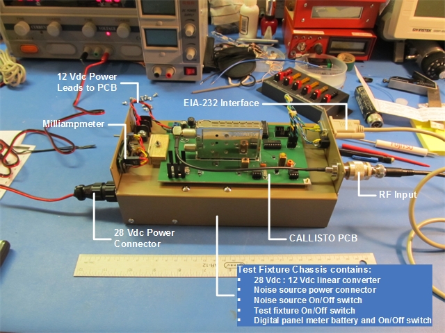
All CALLISTO Solar Radio Spectrometers printed circuit boards (PCB) are tested on a laboratory test fixture. The test fixture is supplied by 28 Vdc, which may be used to power an external noise source through a "hot/cold" switch and BNC connector. It also powers a small step-down linear power supply mounted inside the test fixture chassis. This power supply is adjusted to 12 Vdc for powering the PCB. The test fixture also provides a DB9-F connector for the EIA-232 interface. Click here for layout and schematic drawings associated with the test fixture.
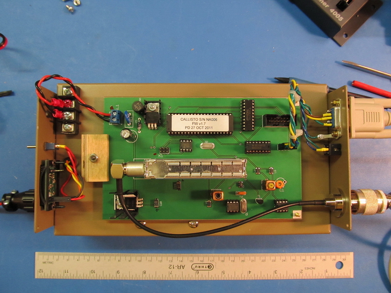
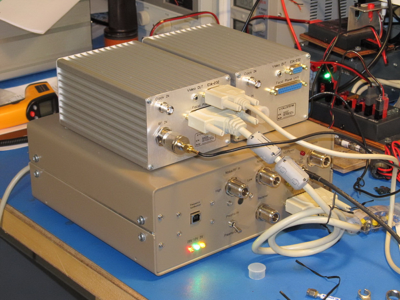
After PCB Assembly, the printed circuit board is installed on the test fixture for preliminary testing and then installed in the enclosure for final testing with a different test fixture shown below. The spectrometer is tested according to the procedures given in the CALLISTO Construction Manual.
The picture immediately below shows a completed PCB in-place for testing. An annotated view of the test fixture alone is provided below.
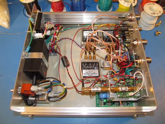
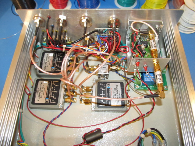
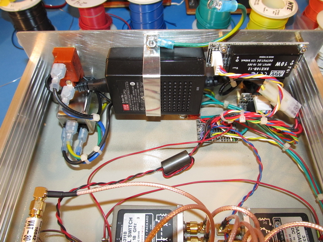
The ready-built and tested versions of the Callisto are tested using automated software procedures and the test fixture shown below.
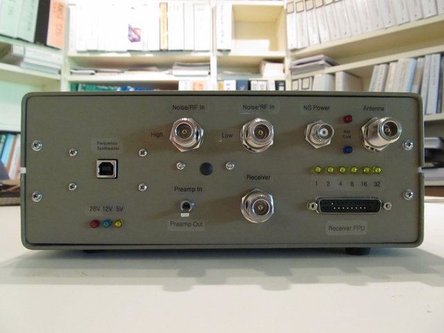
Interior views of test fixture below. The object at the lower-right is a USB-controlled frequency synthesizer before the cover was placed on its enclosure.